Курсовая работа: Bipolar transistors
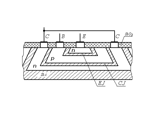
The bipolar transistor terms a three-electrode semiconductor device with two or more interacting electron-hole junction. In the transistor alternate as an electrical conductivity three regions of a semi-conductor, for what in a homogeneous semi-insulating substrate of silicon Si-i the methods of epiplanar technique shape regions of a collector, basis and emitter, (fig. 6.1). For it in a plate Si-n, employee by a collector, the method of a local diffusion (introduction of atoms of doping substance in a chip of a semi-conductor through some part of its surface) forms base region (Si-p). In this region also method of a local diffusion forms emitter region (Si-n) with high density of a donor dopant. On boundary region of emitter with base, and also on boundary of base region with collector are formed two electron-hole (p-n) junctions - emitter and collector (on a title of extreme regions of transistor structure).

Fig. 6.1. Planar n-p-n structure of the bipolar transistor
The junctions appear interacting, if distance between them, called in breadth of basis ![]() , is smaller diffusion lengths of mobile carriers of a charge. The diffusion length
, is smaller diffusion lengths of mobile carriers of a charge. The diffusion length ![]() is a distance, which transits an electron and vacant electron site from a moment of occurrence in a semi-conductor up to a moment of a recombination
is a distance, which transits an electron and vacant electron site from a moment of occurrence in a semi-conductor up to a moment of a recombination ![]() .
.
The area of collector junction always is more than the area of emitter junction. The region of the emitter should have higher electrical conductivity, than basis and collector. An impurity concentration in the region of the transistor owe corresponds as:
![]() . (6.1)
. (6.1)
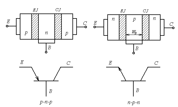
Depending on the order of alternation of regions as an electrical conductivity distinguish structures p-n-p and n-p-n of types.
In a fig. 6.2 the structures p-n-p and n-p-n and their legend on circuitries are shown.

Fig. 6.2. Flat one-dimensional model BT and legends

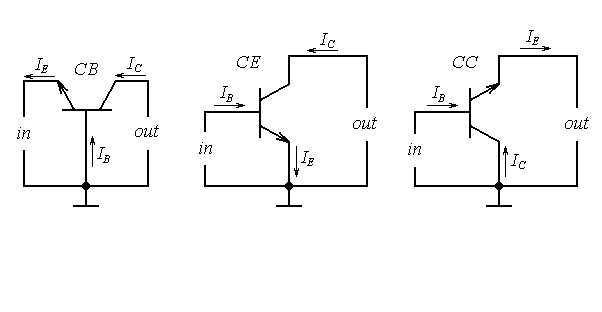
Fig. 6.3. The circuits of insert of bipolar transistors
As a device of an electric circuit, transistor use by such fashion, that one of its electrodes is entering, and another-output. The third electrode is common concerning an input and exit. Depending on what electrode is common, distinguish three circuits of insert of the transistor: common-base (CB), common emitter (CE) and common collector (CC) (fig. 6.3).
6.2. Conditions of insert of the transistor. Static parameters.
Physical processes
By operation of the transistor the voltages from exterior power supplys are affixed to its electrodes. Depending on polarity voltages affixed to electrodes, each of p-n-junctions the transistor can be switched on in direct or in the opposite direction. Four conditions of insert of the transistor are possible.
The table 6.1
| Title of junction | Insert of junction | A title of a condition of insert of the transistor |
EJ CJ | Backward Backward | Condition a splitting contact |
EJ CJ | Direct Direct | Condition of saturation |
EJ CJ | Direct Backward | Fissile condition |
EJ CJ | Backward Direct | Inverse condition |
1. Condition a splitting contact . In a condition a splitting contact both p-n- junction are backswitched on (high-ohmic state of a section E-C). In electrodes of the transistor the thermal currents backswitched of junctions flow past which are static parameters of a condition the splitting contact. In each of three circuits of insert of the transistor these parameters have particular magnitudes. Their labels look like
for the circuit with CB - ![]() ;
;
for the circuit with CE - ![]() ;
;
for the circuit with CC - ![]() ,
,
where the first index means an electrode, in which the current flows past;
the second index – circuit of insert;
the third index - requirement in the rest of the circuit:
о - absence of a current in the other electrode - no-load operation,
s - short-circuit in the rest of the circuit.
2. Condition of saturation. In a condition of saturation both p-n-junctions are directly switched on, the junctions saturated with mobile carriers of a charge, their resistances are small. The section E-C has high conductance and it is possible to consider it short-circuited.
Static parameters are the saturation currents in electrodes the transistor ![]() and residual voltages
and residual voltages ![]() . A voltage ratio and currents relevant electrodes give magnitudes of resistances of saturation:
. A voltage ratio and currents relevant electrodes give magnitudes of resistances of saturation:
 ;
;  .
.
3. Fissile condition . In a fig. 6.4 the flat one-dimensional model of the transistor is shown, which emitter junction is switched on in a forward direction, and collector junction - in backward. Such insert corresponds to a fissile condition, and the transistor has intensifying properties. The principle of operation of the transistor in a fissile condition grounded on use of the following phenomena:
- injection of majority carriers through emitter junction;
- transport of injected carriers through basis owing to diffusions and drift;
- recombination of nonequilibrium carriers in basis;
- extractions of carriers from basis in a collector by a region of collector junction.
The injection of carriers stipulates transiting through emitter p-n-junction of diffusive currents: hole ![]() and electronic
and electronic ![]() .
.
In an external circuit of emitter the current of injection flows past
 , (6.2)
--> ЧИТАТЬ ПОЛНОСТЬЮ <--